Imaging and Microscopy
Imaging is a key application of optics and photonics and CAPPA is engaged in a number of advanced imaging activities. The goal is to gain insight into the structure, form, shape and constituents of the sample under investigation in a non-destructive manner.
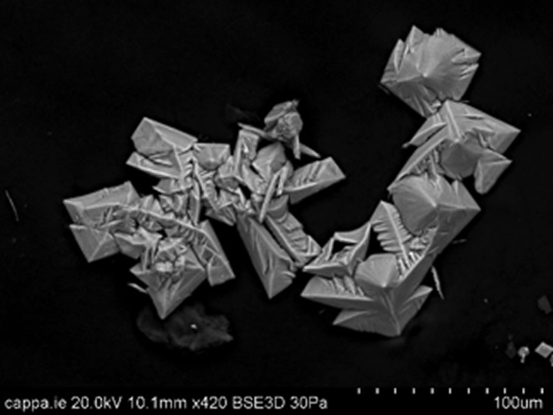
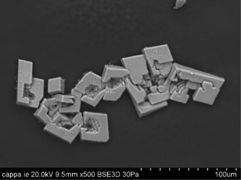
With variable pressure Scanning Electron Microscopy (SEM), non-conducting and water containing samples can be imaged to nanometer resolution. The SEM imaging can be combined with energy dispersive spectroscopy (EDS) to identify and quantify the element constituents of the sample under test. Traditionally, nonconductive samples had to be coated prior to SEM imaging and it was not possible to image wet samples at all. The ability to image nonconductive samples without coating gives CAPPA a great advantage over traditional SEM imaging. Samples can now be imaged in a non-destructive manner and microanalysis can be performed without the influence of carbon or metal coating. The chamber size available can also accommodate large and irregularly shaped specimens. All this flexibility lends itself to imaging samples in their native state. This is ideal for gaining insight into product performance under varying environmental conditions as well as understanding the effect of various process steps and parameters.
By extending the spectroscopic capabilities, CAPPA can also carry out FT-IR and Raman imaging. This technique is often termed Hyperspectral Imaging, Spectroscopic Imaging or Chemical Imaging. This is a powerful combination of FT-IR and Raman Spectroscopy and Microscopy, which yields information on the spatial distribution of the spectral properties within a sample. CAPPA can employ this to investigate the homogeneity of a sample and the distribution of its constituents can be observed. CAPPA can also investigate the form of a surface through interferometric or phase-shifting techniques, which can be design and tailored depending on the sample under test.
Inspection
The first step with all sample analysis is to take a close look at it. In some cases, a quick observation under a microscope can be enough to fulfill the entire project needs. There are many options for lighting, polarization, depth of field and magnification and quickly changing any of these can reveal a surprising amount of information in a short time.
Polarized Light Imaging
Many manufactured goods, especially in the medical device sector, consist of transparent polymers. Polarised light is a rapid method of visualising stress in polymers. Such imaging can be used to help diagnose problems with injection moulding.
Many manufactured goods, especially in the medical device sector, consist of transparent polymers. Polarised light is a rapid method of visualising stress in polymers. Such imaging can be used to help diagnose problems with injection moulding. Polarized Light Microscopy can be used for applications including:
- Identification of Gout Crystals
- Identification of Asbestos Fibers
- Uncovering the History of Rock Formation
- Identification Natural and Synthetic Polymers
Polarizing microscopy provides a vast amount of information about the composition and three-dimensional structure of a variety of natural and synthetic sources. With various application in manufacturing and research, polarizing microscopy is a relatively inexpensive and accessible investigative and quality control tool, which can provide information unavailable with any other technique.
Defect Analysis
The lighting configuration of the microscope is critical to obtaining the desired information. A transmitted light image can be taken only for transparent materials. Light passing through the sample is deflected by the defects and they show as dark spots on a bright background. This can be used to examine defects from the whole depth of the sample, and any features in the background can be blurred out somewhat by manipulating the aperture of light source. The narrow depth of field of the compound microscope can be used to help measure the depth of the defect in the sample.
For surface defects, the best illumination is reflected dark field. Defects on the surface scatter light and only light that is scattered off axis is collected and imaged. This makes it highly sensitive to surface features.


Contamination Identification
The first step with all sample analysis is to take a close look at it. In some cases, a quick observation under a microscope can be enough to fulfil the entire project needs. There are many options for lighting, polarization, depth of field and magnification and quickly changing any of these can reveal a surprising amount of information in a short time. Few samples are completely flat hence to be able to visualise the sample and contamination we need a large depth of filed. Here we see two images of an M6 bolt with various contaminating particles.
The right image is from a stereomicroscope with a long depth of field under bright field polarised light and on the right is from a compound microscope with reflected dark field illumination. Both are able to visualise the red fibre, however the stereomicroscope can locate the fibre and other particles much more quickly to the large depth of field and ability to zoom in and out without swapping objectives. Zooming in further with a stereomicroscope shows that fibre is twisted, indicating it is a natural fibre such as cotton or wool as opposed to a synthetic fibre such as polyester or nylon. Further analysis of this fibre could include SEM imaging or some spectral analysis and matching it with a source fabric. These techniques, require much more time than a quick look with a stereomicroscope and for many projects, this is sufficient information.


