Project Description
COSMICC

Project Description
In COSMICC, the Nanophotonics group is working with key industrial and research partners in the fields of Silicon Photonics, CMOS electronics, Packaging, Optical transceivers and Data centres. The project goal is to demonstrate that mass commercialisation of Silicon photonics based transceivers is possible by 2019 through the enhancement of the existing photonic integration platform at ST-Microelectronics. COSMICC will develop optical transceivers that will be packaged on-board and by combining CMOS electronics and Si-photonics with innovative high-throughput fibre-attachment techniques, the developed solutions will be highly scalable. With performance improved by an order of magnitude as compared with current VCSELs transceivers, the COSMICC technology will answer tremendous market needs with a target cost per bit that the traditional WDM transceivers cannot meet. The early setting up of a new value chain will enable exploitation of the developed technologies.
About COSMICC Research
This project has received funding from the European Union Horizon 2020 Programme,
under grant agreement number 688516.

Consortium
In order to reach these ambitious objectives the consortium consists of eleven partners from both industry and academia in five European countries. Munster Technological University is represented by Dr William Whelan-Curtin, the nanophotonics group leader at CAPPA. He co-founded and runs NanoPIX, a foundry service for the nanophotonic devices, which has supplied 15-20 research teams across Europe with bespoke samples, resulting in more than 80 joint publications since September 2006.


Approach
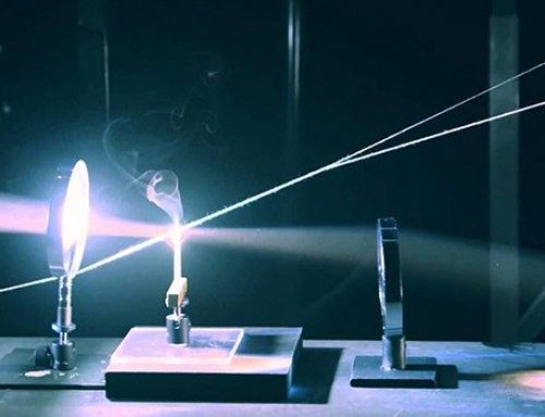
In the first high reward step-modification of the fabrication platform, COSMICC consortium will achieve mid-board optical transceivers in the [2Tbit/s-2pJ/bit-0.2€ per Gbit/s]-class with ~200Gbit/s per fiber: the introduction of one process brick (SiN layer) in the photonic process will enable low-cost packaging techniques (up to 2 x 12 fiber channels) and practical coarse WDM implementation (4 wavelengths with no temperature control requirements.) The built demonstrators will be tested in lab and field environments. In compliancy with the enhanced fabrication platform, lasers will be developed by heterogeneous integration of III-V material, targeting improved temperature behaviour, and doubled-bit-rate payback. A second step-modification of the fabrication will consist in evaluating a disruptive process that enables SiGe layers with tunable Si-composition for achieving micrometer-scale devices.