
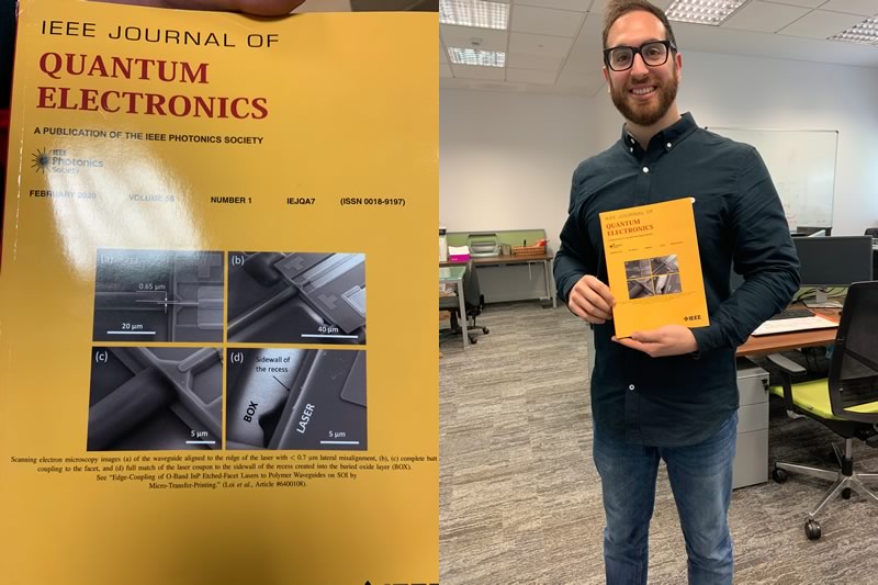
The Centre for Advanced Photonics and Process Analysis (CAPPA) was delighted to have their researcher Simone Iadanza’s work recently published on the cover of the IEEE Journal of Quantum Electronics, with images from a publication, which was titled “Edge – Coupling of O – Band InP Etched – Facet Lasers to Polymer Waveguides on SOI by Micro – Transfer – Printing.”
The IEEE Journal of Quantum Electronics is a monthly peer reviewed scientific journal, covering optical, electrical and electronic engineering, and some applied aspects of lasers, physical optics and quantum electronics. It is published by the IEEE photonics society and was established in 1965.
O-band InP etched facets lasers were heterogeneously integrated by micro-transfer-printing into a 1.54 μm deep recess created in the 3 μm thick oxide layer of a 220 nm SOI wafer. A 7 × 1.5 μm 2 cross-section, 2 mm long multimode polymer waveguide was aligned to the ridge post-integration by e-beam lithography with <; 0.7 μm lateral misalignment and incorporated a tapered silicon waveguide. A 170 nm thick metal layer positioned at the bottom of the recess adjusts the vertical alignment of the laser and serves as a thermal via to sink the heat to the Si substrate. This strategy shows a roadmap for active polymer waveguide-based photonic integrated circuits.
You can read the full paper here and you can learn more about the research CAPPA is currently involved in here.